|
Modifying the Quartex Radio Controlled
Clock module

Figure 1 shows the Quartex module partially disassembled.
The Battery + connection is closest to the inside cutout.
|
Be careful removing the ferrite antenna and it's
associated tank
capacitor
from the plastic enclosure. The factory used a strong contact cement
to
hold it in place, making their removal difficult without breaking wires
or
damaging the ferrite bar antenna.
If you have already damaged some parts:
Stop now. Go find a new hobby!
I have completely disassembled the radio clock module,
and prepared
it
for the modification procedures that follow.

Figure 2
Figure 2 shows the disassembled Quartex module, with the
movement,
switch, and speaker removed from the PCB assembly. The movement
and switch will not be used, and can be discarded. Next, you
will need
to cut down the PCB to fit, and then drill six holes for parts and
wiring.
|
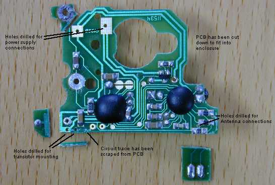
Figure 3
Figure 3 shows the receiver PCB cut down to fit into the
small enclosure.
Six holes were drilled through the PCB
to accomodate the additional parts, and wiring connections. I
cut the PCB using sidecutters, then dressed the edges
with a file. The holes were drilled using a small hand drill. The holes
for the transistor leads, and power supply cable
were made using a 0.032" bit. The two antenna connection holes were
drilled using a 0.022" bit. The unused copper
traces that connected to the antenna pads were scraped off, also the
trace connecting the predrilled pad to ground by
the transistor mounting position was removed to accomodate the 10k
resistor.
|
Below, the PCB is shown at an angle to help
you understand the installation of the 2N3904
transistor used as a buffer for the reset circuit.
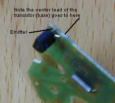
Figure 4
Figure 4 shows the 2N3904 transistor mounted
on the component side of the PCB. The Collector
lead is inserted into the existing pushbutton switch
hole, the Emitter lead is inserted into the newly
drilled hole below the Collector, and the Base lead
is inserted into the newly drilled hole offset from
the other two.
|
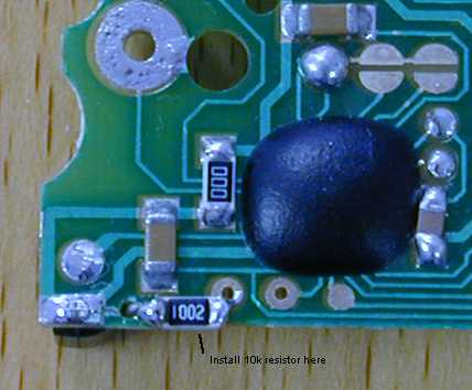
Figure 5
Figure 5 shows the detail of the installed 2N3904
transistor, and 10k
resistor on the PCB.
A 1206 package surface mount resistor was used. You can also use an
0805 package.
Do take care in soldering the transistor's Base lead to the resistor,
it is very close to the
existing decoupling capacitor on the PCB. This completes the reset
circuit modification.
|
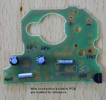
Figure 6
The PCB component side was marked with the wiring
connections to ease
the final assembly. Note the two antenna connection holes at far left
for
connection to the ferrite antenna. The antenna wires are not polarized.
|
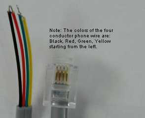
Figure 7
|
Figure 7 shows the two ends of the four conductor
telephone wire,
and the RJ14
connector. Note the color sequence of the connector with the locking
tab towards
the bottom. It should be Black, Red, Green, and Yellow. The receiver
must be
wired using this color sequence if the colors are used to determine
the connection
at the RJ14 connector. TheWWVB clock PCB uses the following wire
assignment:
Black =
Ground
Red = 1.5v
+
Green = 1PPS output
Yellow = Reset input
|
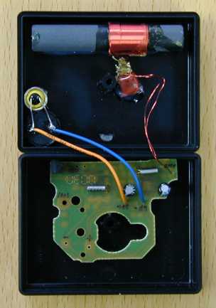
Figure 8
Figure 8 shows all of the parts positioned in the case.
The Piezo
buzzer was mounted in the lid of the case using CA glue. A small
hole was drilled in the lid, the same diameter as the hole in the
buzzer, to allow the sound to pass through.
The Antenna and tank capacitor were glued into the lid
of the case
using household RTV sealant. A small amount of RTV was applied
to the PCB to secure it after soldering the phone wires in place.
|
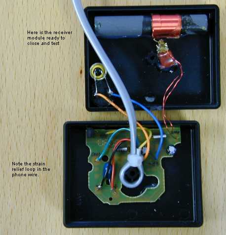
Figure 9
A 2.2uf Tantalum capacitor was soldered into the battery
connection
holes. The capacitor serves
to decouple the supply, and reduce the effect of transients. Any
capacitor
value between 1 and 4 uf
can be used here. A smaller value will take less time to discharge,
allowing a faster clock restart.
A strain relief loop in the phone cable helps avoid damage. A small
slot was filed into the two case
halves to permit the wire to pass without being pinched.
|
Click
here to return to the Radio Controlled Nixie Clock site
|